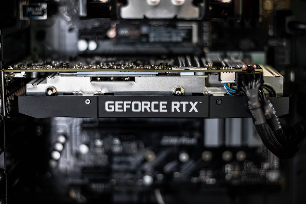
Where Does NVIDIA Make Its GPUs?
In the blazing core of the AI revolution, NVIDIA reigns as the undisputed architect of accelerated computing, its GPUs the beating heart of everything from ChatGPT’s whispers to autonomous fleets’ vigilant eyes.
Since Jensen Huang’s garage-born vision in 1993, the Santa Clara sentinel has sculpted over 80% of the AI training market, with Blackwell’s GB200 Superchips, packing 208 billion transistors and 30x the inference speed of Hopper, fueling a $3 trillion valuation spike in 2025 alone.
These silicon symphonies, etching exaflops into wafers thinner than a hair, power hyperscale data centers gobbling gigawatts while gaming rigs chase ray-traced realms.
But where does this transistor titan forge its forbidden fruit?
NVIDIA’s alchemy is a fabless fantasia: designs dazzle in California, but fabrication dances across Taiwan’s fabs, Korea’s kilns, and America’s awakening assembly halls.
Hsinchu Science Park
In the bamboo-shaded brain trust of Hsinchu, TSMC’s gleaming gigafabs, spanning 20+ sites like Fab 18 and Fab 21, birth 90% of NVIDIA’s elite GPUs, from GeForce RTX 5090s to DGX GB200 racks.
- Key Role: Wafer fabrication on 3nm/2nm processes; CoWoS advanced packaging stacking HBM3e atop Blackwell dies for 8TB/s bandwidth.
- Scale: 50,000+ engineers in 10 million square feet, etching 100,000 wafers monthly, each Blackwell GPU demands a custom interposer, yielding 1.4 million chips quarterly at peak.
- Precision Pulse: Liquid-cooled cleanrooms hum at 100 particles per cubic meter, with EUV lithography from ASML blasting patterns 100,000x finer than a virus.
Giheung Campus
Nestled in Yongin near Seoul, Samsung’s 1,000-acre empire, anchored by Fab S3 for 3nm trials, supplies 10-15% of NVIDIA’s mid-tier GPUs and all HBM stacks, the high-bandwidth memory turbocharging AI inference.
- Key Role: HBM3E fabrication (12-layer stacks hitting 1.2TB/s); select Blackwell packaging via I-Cube 2.5D tech.
- Scale: 30,000 workers across 5 million square feet, producing 500,000 HBM modules daily, NVIDIA’s Q3 2025 order: 2 million units for GB200 NVL72 racks.
- Edge Evolution: Passed NVIDIA qual in August 2025, edging out Micron for cost-competitive cobalt-doped DRAM.
Phoenix Fab Cluster
In the Sonoran sands, TSMC’s $65 billion bet, Fabs 21/22 online since Q1 2025, marks NVIDIA’s first U.S.-born Blackwells, dodging duties with domestic dazzle.
- Key Role: 4nm/3nm wafer fab for RTX consumer GPUs; initial GB200 packaging via Amkor/SPIL outposts.
- Scale: 6,000 workers (ramping to 20,000) in 1 million square feet, yielding 20,000 wafers monthly—first Blackwell batches shipped April 2025.
- Resilient Reveal: Water-recycled from the Salt River, these quake-proof quads cut latency for U.S. hyperscalers like Oracle.
Houston & Dallas Superfactories
In the Lone Star sprawl, NVIDIA’s $500 million duo commissions rack-scale wonders, from HGX B200 boards to liquid-cooled NVL72 behemoths.
- Key Role: GB200 Superchip assembly; NVLink integration and burn-in testing for 72-GPU domains.
- Scale: Foxconn Houston (1M sq ft, 5,000 jobs) and Wistron Dallas (800K sq ft) targeting 10,000 racks annually by Q4 2026.
- Trailblazer Twist: Mass production ramps Q2 2026, with GR00T robots auditing yields at 99.9%.
NVIDIA’s designs dazzle in Santa Clara’s sunlit labs, but a 2,500-supplier swarm spans continents for lithography lenses and cobalt cathodes.
Snapshot of the silicon syndicate:
| Location | Role | Notable Contributions |
|---|---|---|
| Veldhoven, Netherlands (ASML) | Lithography | EUV machines etching 2nm features; 100% of Blackwell exposure. |
| Ibiden, Japan | Substrates | Organic interposers for CoWoS; 70% NVIDIA share. |
| SK Hynix, South Korea | HBM Memory | 80% of GB200’s 192GB stacks; yield hits 85% in 2025. |
| Amkor/SPIL, Arizona/Philippines | Packaging/Testing | Post-fab encapsulation; 500K dies/month for U.S. lines. |
| Dow/DuPont, USA | Materials | Insulators and underfill epoxies for thermal resilience. |
This lattice, 60% Asian, 25% U.S., navigates HBM shortages with SOCAMM trials, boasting 40% recycled rare earths in 2025 GeForces.


