Where Does AMD Make Its Chips?
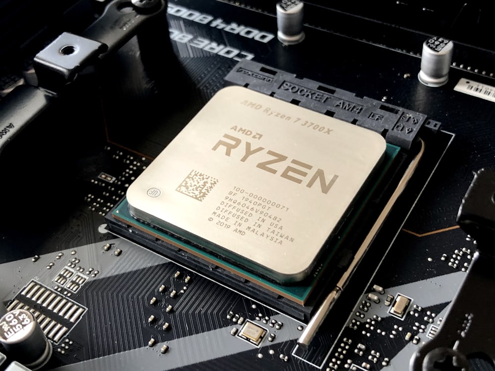
In the electrified epicenter of computing’s core, AMD surges as the silicon underdog turned titan, its CPUs and GPUs the pulse of AI infernos and gaming galaxies alike.
From the Ryzen 9000’s Zen 5 zenith, packing 16 cores at 5.7 GHz with AI-etched efficiency, to the MI400’s monstrous 288GB HBM3e stacks powering OpenAI’s six-gigawatt odyssey, AMD’s silicon scripts the scripts of tomorrow.
Over 40% server CPU share by mid-2025, eclipsing Intel’s throne, with RDNA 4’s Radeon RX 9070 XT unleashing 20% rasterization leaps at 4nm finesse. These transistor tapestries, denser than a neural net’s dream, propel hyperscalers from xAI’s Colossus to Xbox’s quantum quests.
But where does this fabless phenom forge its forbidden fruit?
AMD’s alchemy is a foundry fantasia: blueprints blaze in California, wafers whisper in Taiwan, and packages pulse across Asia’s archipelago.
Hsinchu Science Park
In the innovation incubator of Hsinchu, home to Fab 18’s EUV empires and Fab 21’s 3nm odysseys, TSMC crafts AMD’s crown jewels, from Zen 5 CCDs to RDNA 4’s compute colossi.
- Key Role: Wafer fabrication on 5nm/4nm/3nm processes; chiplet stacking for MI400’s 2.2x inference surge over MI300X.
- Scale: 60,000+ engineers across 12 million square feet, slicing 150,000 wafers monthly, each Ryzen 9950X demands dual CCDs, yielding 2 million consumer dies quarterly at 95% yields.
- Finesse Forge: Helium-cooled cleanrooms hum at 10 particles per cubic meter, with ASML’s High-NA EUV lasers inking features 70,000x finer than a bacterium.
Phoenix Fab 21
Amid Sonoran saguaros, TSMC’s $65 billion desert dominion, Phase 1 humming since Q1 2025, births AMD’s first all-American Ryzen 9000 dies, a tariff-taming triumph.
- Key Role: 4nm wafer fab for Zen 5 consumer CPUs and MI400 HPC accelerators; initial CoWoS packaging trials with Amkor.
- Scale: 8,000 workers (scaling to 25,000) in 1.2 million square feet, outputting 25,000 wafers monthly, first EPYC Turin batches shipped July 2025, slashing logistics latency by 40%.
- Resilient Radiance: Aquifer-replenished ops recycle 80% water, these quake-quelling quads cut supply risks for U.S. datacenters like Microsoft’s Azure.
Phoenix’s pivot, pollinated by $52 billion in federal fertilizer, heralds “Made in USA” for 15% of AMD’s output by 2026, fueling Pentagon pacts and OpenAI’s stake play.
Giheung Campus
In Yongin’s verdant valleys near Seoul, Samsung’s sprawling 1,200-acre arsenal, Fab S5 for 4nm forays, handles AMD’s mobile and embedded envoys.
- Key Role: 4nm/5nm production for Ryzen AI 300 APUs and Radeon 7040M iGPUs; HBM-lite stacks for edge AI.
- Scale: 35,000 staff across 6 million square feet, fabricating 400,000 dies daily, AMD’s Q3 2025 allocation: 500,000 units for laptop legions.
- Adaptive Alloy: GAAFET gates boost density 20% over FinFET, with cobalt-infused interconnects curbing electromigration.
Giheung’s geothermal guardians, grooved by Gangnam’s glow, export via Incheon, a 5% hedge as AMD reportedly reroutes 4nm EPYC orders to Arizona in May 2025.
AMD’s designs dazzle in Santa Clara’s sun-drenched labs, but a 1,800-supplier swarm spans spheres for lithography lenses and lanthanum lasers.
Snapshot of the silicon syndicate:
| Location | Role | Notable Contributions |
|---|---|---|
| East Fishkill, New York (GlobalFoundries) | Legacy Fabs | 12nm I/O dies for older Ryzen; $2.1B wafer pact through 2025 for specialty SoCs. |
| Dresden, Germany (GlobalFoundries) | RF/Analog | 22FDX for wireless modems; EU’s “Trusted Foundry” for secure edge chips. |
| Penang, Malaysia (AMD/TF AMD) | Assembly/Test | Chiplet packaging for 50% of Ryzen; new $135M lab ramps R&D in Bayan Lepas. |
| Kaohsiung, Taiwan (ASE) | Advanced Packaging | 2.5D interposers for MI400; 2.5x compute boost via EPYC standardization. |
| Suzhou, China (ASE) | Volume Assembly | Radeon RX consumer GPUs; 30% of global test capacity amid U.S. diversification. |
This matrix, 70% Asian, 20% U.S./EU, navigates node famines with multi-sourcing, boasting 35% recycled cobalt in 2025 Instincts.